
Etch and Deposition Processes for BioMEMS Manufacturing
BioMEMS is an exciting area of the MEMS market, and SPTS offers a range of wafer processes which enable development and commercial manufacturing of BioMEMS
DownloadBioMEMS is an exciting area of the MEMS market, with growing numbers of products now coming to market after many years of research. Key applications for BioMEMS may fall under medical/pharmaceutical, food safety or environmental/public safety monitoring. According to Yole Développement[1], “With the addition of microfluidic chips (Si-based, polymer-based, glass-based), the BioMEMS market, represented by silicon MEMS devices used for life sciences and healthcare applications, is expected to more than double - from $3B in 2017 to $6.9B in 2023, with a CAGR of 14.9% from 2017 – 2023”.
Microfluidic chips are the predominant MEMS structure utilized, but there are also biomedical applications for optical MEMS and MEMS sensors (e.g. measuring flow, gas, motion and pressure). There are now many BioMEMS products on the market, and more at various stages of development.
There are multiple drivers for the miniaturization of medical devices, such as:
BioMEMS can be made of a number of different materials. Historically silicon was the most popular due to established micromachining technology and easy integration with control electronics. However, bulk silicon is not biocompatible[2] and can cause reaction with living tissue if implanted in-vivo, so other materials like inert metals, glass or polymers (e.g. PDMS, Parylene or PMMA) are also important in BioMEMS.
Glass is transparent and has good strength and chemical inertness, but is more difficult/expensive to micromachine in mass production. Polymers are cheap and easy to mass-manufacture, and in certain cases are transparent and biocompatible. However they are generally weaker and may deform under certain conditions, they usually have poor high temperature tolerance and are more difficult to integrate with electronic control.
Piezomaterials like PZT or AlScN have the very useful property of generating an electrical charge when stressed, or conversely deforming on application of an electric signal. These materials are used in BioMEMS applications such as micropumps, ultrasonic imaging, smart catheters, and energy harvesting devices. It should be noted that lead-containing PZT is not suitable for implanted devices, so researchers are investigating alternatives like scandium-doped AlN which is biocompatible.
In all these examples, material choice will vary depending on the specific requirements of the particular application. As a key supplier to the MEMS industry, SPTS has been supporting researchers and biomedical companies for many years. The following examples illustrate some of our most recent collaborations, developing a variety of BioMEMS.
Silicon BioMEMS usually involve etching vertical holes or trenches typically >100 µm deep into the silicon, using the well-established Deep Reactive Ion Etching (DRIE). As a pioneer of this technique since its invention in the mid- 1990’s, SPTS continues to offer market-leading Si DRIE technology with high etch rates and excellent tilt and sidewall control. One on-going project, with Swansea University, is focused on manufacturing hollow, tapered silicon microneedles for transdermal fluid sampling, drug delivery and vaccine delivery[3]. SPTS Si DRIE is also being used at imec for micromachining silicon to create the “Neuropixels” neural probe[4] which contains almost 1000 CMOS sensors on a thin silicon (L)1cm x (W)70µm x (H)20µm probe for recording the electrical activity of neurons across the brain.
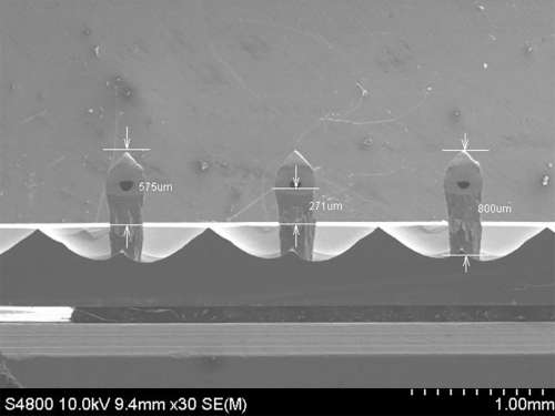
Silicon microneedles
(Courtesy of University of Swansea)
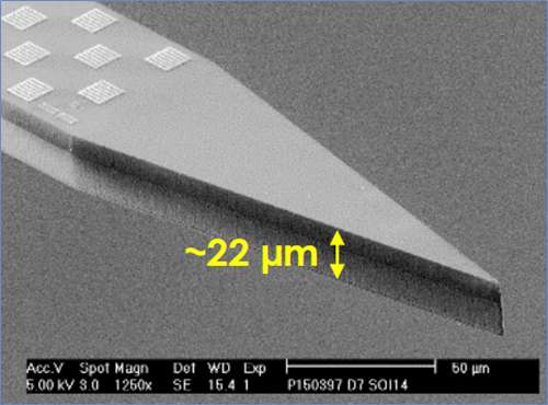
DRIE-etched silicon “Neuropixels” neural probe
(Courtesy of imec)
In a recent joint paper with imec[5], we illustrated how our Synapse system could be used to etch smooth microchannels in quartz. When etching 20µm wide microfluidic channels using a photoresist mask, we achieved an aspect ratio of 2.1:1 (Etch Rate ~0.4µm/min) and with an aluminium mask the aspect ratio rose to >3.8:1, with an etch rate of ~0.5µm/min. Using SPTS’s Molecular Vapor Deposition (MVD) technology, the glass microchannels were coated with 3-[Methoxy(polyethyleneoxy)propyl] trimethoxysilane, resulting in a static advancing contact angle of 40.5˚ for water passing through the microchannel. In this work, the quartz microchannels were used to hold a serum containing human red-blood cells, for imaging/cell counting. Therefore the smoothness of the etched channel surface was critical to allow clear, high resolution imaging.
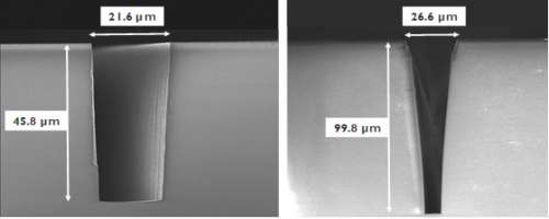
Deep quartz microchannel etch using (a) 14µm deep PR mask and (b) 5µm deep Al mask
SPTS also contributed to the EU-funded InfoMed Project[6], a large consortium of 39 organisations and companies, involved in establishing an integrated pilot line for medical devices, developing scalable processes and demonstrating various products. One demonstrated product named “Cytostretch”, developed by TU Delft and being transferred to production, involved combining induced pluripotent human stem cells with a stretchable multi-electrode array to mimic the physical in-vivo environment for more realistic and cost-effective testing of drugs. As part of this project, SPTS developed a dry ICP etch process for PDMS, with an etch rate of ~1.8µm/min and cross-wafer uniformity of 1.7[DB2] %.
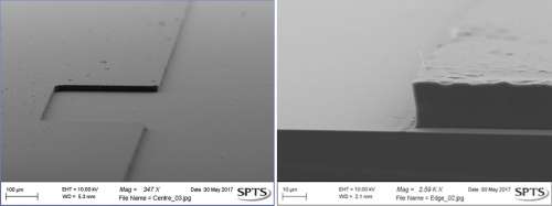
ICP etched PDMS
For more details about the SPTS process solutions used for BioMEMS manufacturing, email us, or fill in the Contact Form. For further product information, click the links below:
References
[1] “BioMEMS & Non-Invasive Sensors: Microsystems for Life Sciences & Healthcare 2018” Report by Yole Développement, August 2018 (https://www.slideshare.net/Yole_Developpement/biomems-noninvasive-sensors-microsystems-for-life-sciences-healthcare-2018-report-by-yole-developpement)
[2] “Is Silicon Suitable for Making Implantable Biomedical Devices” Anfeng Wang et al. Presented at AIChE Annual Meeting 2005 (https://aiche.confex.com/aiche/2005/techprogram/P15420.HTM)
[3] "Advanced deep reactive-ion etching technology for hollow microneedles for transdermal blood sampling and drug delivery" Liu, Y., Ashraf, H., Roberts, K., Knight, N., Eng, P. & Guy, O. (2013). . IET Nanobiotechnology 7(2), 59-62.
[4] “Fully integrated silicon probes for high-density recording of neural activity”, James J Jun et al, Nature, volume 551, p232–236 (November 2017)
[5]“Microfluidics on 200mm Quartz Substrates using Semiconductor Fab Dry Etch Process as an Enabler for Imaging Applications in Life Sciences” Andim Stassen et al, presented at MNE 2017, Braga Portugal (Sept 2017)
[6] http://informed-project.eu/
Information on this page contains forward looking information. For more information, click here: https://www.orbotech.com/fls
The link you have selected is located on another server. Neither SPTS Ltd. nor any of its subsidiaries endorses this web site, its sponsor, or any of the information, policies, activities, products, or services offered on the site or by any advertiser on the site. By clicking on the OK button below, you agree and acknowledge the foregoing and will be directed to the selected site.